
The concept was until now purely theoretical. First predicted in 1934 by
Eugene Wigner, this structure - commonly referred to as the “Wigner crystal” -
would be made up exclusively of electrons, positioned in such a way that they
do not repel each other and remain stable. This is the first time that
scientists have created and managed to image such a crystal.
If the conditions are just right, some of the electrons inside a material
will arrange themselves into a tidy honeycomb pattern — like a solid within
a solid. Physicists have now directly imaged these ‘Wigner crystals’, named
after the Hungarian-born theorist Eugene Wigner, who first imagined them
almost 90 years ago.
Researchers had convincingly created Wigner crystals and measured their
properties before, but this is the first time that anyone has actually taken
a snapshot of the patterns, says study co-author Feng Wang, a physicist at
the University of California, Berkeley. “If you say you have an electron
crystal, show me the crystal,” he says. The results were published on 29
September in Nature.
A structure conducive to the appearance of the phenomenon
To create the Wigner crystals, Wang’s team built a device containing
atom-thin layers of two similar semiconductors: tungsten disulfide and
tungsten diselenide. The team then used an electric field to tune the
density of the electrons that moved freely along the interface between the
two layers.
In ordinary materials, electrons zoom around too quickly to be significantly
affected by the repulsion between their negative charges. But Wigner
predicted that if electrons travelled slowly enough, that repulsion would
begin to dominate their behaviour. The electrons would then find
arrangements that minimize their total energy, such as a honeycomb pattern.
So Wang and his colleagues slowed the electrons in their device by cooling
it to just a few degrees above absolute zero.
A mismatch between the two layers in the device also helped the electrons to
form Wigner crystals. The atoms in each of the two semiconductor layers are
slightly different distances apart, so pairing them together creates a
honeycomb ‘moiré pattern’, similar to that seen when overlaying two grids.
That repeating pattern created regions of slightly lower energy, which
helped the electrons settle down.
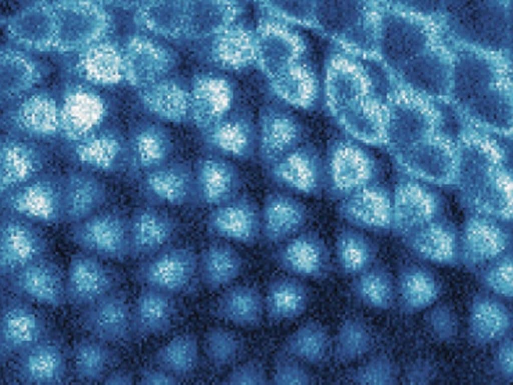
Images obtained using a carbon sheet
The team used a scanning tunnelling microscope (STM) to see this Wigner
crystal. In an STM, a metal tip hovers above the surface of a sample, and a
voltage causes electrons to jump down from the tip, creating an electric
current. As the tip moves across the surface, the changing intensity of the
current reveals the location of electrons in the sample.
Initial attempts to image the Wigner crystal by applying the STM directly on
the double-layer device were unsuccessful, Wang says, because the current
destroyed the fragile Wigner arrangements. So the team added a layer of
graphene, a single-atom sheet of carbon, on top. The presence of the Wigner
crystal slightly changed the electron structure of the graphene directly
above, which was then picked up by the STM. The images clearly show the neat
arrangement of the underlying Wigner electrons. As expected, consecutive
electrons in the Wigner crystal are nearly 100 times farther apart than are
the atoms in the semiconductor device’s actual crystals.
“I think that’s a great advancement, being able to perform STM on this
system,” says Carmen Rubio Verdú, a physicist at Columbia University in New
York City. She adds that the same graphene-based method will enable STM
studies of a number of other interesting physical phenomena beyond Wigner
crystals. Kin Fai Mak, a physicist at Cornell University in Ithaca, New
York, agrees. “The technique is non-invasive to the state you want to probe.
To me, it is a very clever idea.”
Reference:
Li, H., Li, S., Regan, E.C. et al. Imaging two-dimensional generalized Wigner
crystals. Nature 597, 650-654 (2021).
DOI: 10.1038/s41586-021-03874-9
Tags:
Physics